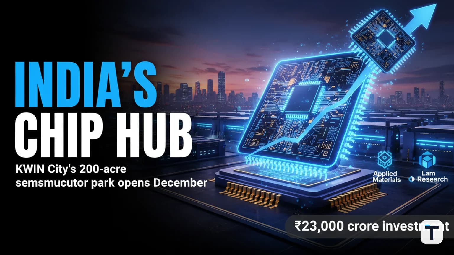

Karnataka's 200-acre semiconductor park — in Phase I of Knowledge, Wellbeing and Innovation (KWIN) City, north-west of Bengaluru — becomes operational in December 2026. The announcement was made by M.B. Patil, Minister for Large and Medium Industries, at the 15th Strategic Electronics Summit on 23 July 2026, alongside a pivot away from tier-1 Bengaluru overstretch and towards an integrated "design-to-export" value chain none of the competing Indian chip clusters has yet assembled.
The headline number is ₹23,000 crore in state-approved semiconductor and Electronics System Design and Manufacturing (ESDM) investments, committed two years ago and now timed to land at roughly the same moment the park opens. Three anchor tenants — Applied Materials India (₹4,851 crore), Lam Research (₹15,901 crore), and Bharat Semi Systems (₹2,342 crore) — are expected to create more than 3,500 high-skilled engineering jobs. Below we break down what each tenant actually builds, why the December deadline is real but fragile, and how the park plugs into the single largest coordinated industrial play any Indian state has staged in semiconductors.
What KWIN City actually is, in one paragraph
KWIN City — the acronym stands for Knowledge, Wellbeing, and INnovation — is a 5,800-acre township being developed by the Karnataka Industrial Areas Development Board (KIADB) between Doddaballapur and Dabaspet, roughly 45 minutes from Kempegowda International Airport. Earlier known as KHIR (Knowledge, Health, Innovation & Research) City, it was repositioned and inaugurated by Chief Minister Siddaramaiah in September 2024 as a parallel city designed to absorb the overflow of Bengaluru's saturated core. The 200-acre semiconductor park sits inside Phase I of that township, which is the slice the state is delivering first; the wider KWIN build-out will be phased over several years.
The reason the semiconductor park matters more than a generic industrial estate is that it is the first Indian site specifically zoned with shared cleanrooms, bulk power, bulk water, and hazardous-waste handling tailored to wafer fabs and OSAT (Outsourced Semiconductor Assembly and Test) facilities, rather than being retrofitted into land that was originally planned for something else. That pre-engineering is what lets the December deadline be plausibly operational rather than a press-release ribbon-cutting on an empty field.
The three anchor tenants, side by side
What separates this park from every other Indian semiconductor announcement in 2026 is the mix of the three anchor tenants. They are not three identical fabs — they span equipment R&D, OSAT-adjacent silicon-component manufacturing, and full-value-chain design. That breadth is what creates the MSME supplier demand the minister is banking on.
Applied Materials India — ₹4,851 crore. An R&D fab and an India Centre for Semiconductor Manufacturing (ICSM) on roughly 10 acres. The formal scope is process engineering, equipment engineering, and a materials lab. This is the part of the park that is closer to a research campus than a volume production fab — it lets the company design the tooling Indian fabs will eventually buy.
Lam Research — ₹15,901 crore. Split across two streams: a ₹6,790 crore R&D lab (silicon etch process development, focused on advanced nodes including 2 nm-class) and a ₹9,111 crore silicon-component manufacturing line. This is the single largest private commitment at the park and the most globally consequential — Lam is the world's second-largest semiconductor-equipment maker, and its willingness to manufacture in India is the clearest signal yet that the domestic supply chain is moving past proof-of-concept.
Bharat Semi Systems — ₹2,342 crore. The domestic anchor — full chain from chip design to OSAT packaging and final test. Roughly 600 jobs. If Applied Materials and Lam are the gravity sources attracting global component suppliers, Bharat Semi is the proof point that an Indian-owned firm can occupy the design-to-OSAT value chain in the same park, on the same shared cleanroom infrastructure.
| Anchor tenant | Investment | What they build | Approx. jobs | Role in the park |
|---|---|---|---|---|
| Applied Materials India | ₹4,851 crore | R&D fab + ICSM materials lab | ~1,500 | Equipment and process engineering — the R&D gravity source |
| Lam Research | ₹15,901 crore | R&D lab (2 nm-class etch) + silicon-component manufacturing line | ~1,400 | Global equipment-maker's first India manufacturing footprint |
| Bharat Semi Systems | ₹2,342 crore | End-to-end design to OSAT packaging and test | ~600 | Domestic anchor proving the design-to-OSAT chain works here |
The three tenants together cover what M.B. Patil described as the state's ambition for companies "to undertake the entire value chain within the State — from design and development to prototyping, testing, certification and exports." Applied Materials owns the equipment R&D layer, Lam owns the silicon-component manufacturing layer, Bharat Semi owns the OSAT end of the chain — and the MSME integration plan means local suppliers feed all three.
Why the December deadline is real — but fragile
Two things make the December 2026 operational target credible in a way past Indian chip-project deadlines have not been. First, the investments were approved by the cabinet sub-committee chaired by Chief Minister Siddaramaiah on 29 May 2025 — not last month — so the anchor tenants have already been through Karnataka's single-window approval process, which now integrates 42 departments and 110 government services. Second, the semiconductor park's shared infrastructure (cleanrooms, bulk power, water recycling, hazardous-waste handling) was specified for semiconductor use at the zoning stage, which is the single hardest unbottleneck to retrofit on a generic industrial estate.
The fragility is still visible, though. An "operational by December" headline tells you the park will have power, water, and cleanroom shell ready; it does not tell you that a 2 nm-class etch line is producing wafers the same month. India's semiconductor track record — from the long-pending Gujarat fab proposals to the Tamil Nadu semiconductor clusters at Cheyyar and Marakkanam — is littered with parks that opened ceremonially and then took years to reach first-wafer. The honest read on the December deadline is: infrastructure will be ready, anchor tenants will be on-site, but the supply chain will still be assembling itself through 2027 and into 2028.
The converging stack no other Indian state has matched
What makes the KWIN City chip park genuinely different from the dozen-odd semiconductor and electronics clusters announced across India in 2026 is not the park itself — it is the convergence of three separately large bets being staged on the same north-Bengaluru axis at the same time. Each of these stacks is independently large. Karnataka is the only state stacking them together.
1. The semiconductor park (this story)
The 200-acre, three-tenant, ₹23,000-crore park covered above.
2. India's first government-driven AI university
On 14 July 2026, Chief Minister D.K. Shivakumar announced a government-driven AI university — the first in India to be state-funded rather than private — with an incubation hub, an agriculture-AI focus, an indigenous foundation-models programme, and a stated alignment with the central IndiaAI Mission. The university is not formally inside KWIN City, but it is geographically and strategically adjacent, and it is the single biggest reason the KWIN semiconductor park can credibly claim a pipeline of indigenous talent rather than imported-only engineers. Karnataka already produces more than 1 lakh (100,000+) engineering graduates a year from 250 engineering colleges, and hosts over 900 Global Capability Centres (GCCs) — the talent floor for any semiconductor cluster is already the deepest in India. The AI university is the bolt-on that lets a local chip designer move from an engineering degree to an applied-AI role at the same firm without leaving the corridor.
3. Beyond Bengaluru — the tier-2 cluster programme
The KWIN chip park does not exist in isolation. It sits atop Karnataka's wider Beyond Bengaluru cluster programme, which is deliberately distributing technology investment across Mysuru, Mangaluru, Hubballi-Dharwad, Shivamogga, Kalaburagi, and Tumakuru to stop Bengaluru's saturation from throttling the next decade of growth. The semiconductor park draws the headline investments; the tier-2 clusters provide the cost-arbitrage back office — Mysuru's forthcoming PCB park, the 235-acre EMC 2.0 cluster, the Tamil Nadu electronics cluster precedent at Cheyyar, and Tumakuru's National Investment and Manufacturing Zone together assemble a multi-tier supply chain where a Bengaluru-headquartered chip designer can source a PCB from Mysuru, a pressed-steel fab fitting from Hubballi, and still be within a 90-minute air or truck hop of every supplier.
The three stacks converging on one timeline — park, AI university, tier-2 clusters — is the thing to watch. It is also why this story is not just a Bengaluru-story.
What builders, MSMEs, and investors should actually do
Park openings are about supply chains, not opening ceremonies. If you are a supplier, a builder, or an investor evaluating whether this park is a real opportunity, the decision framework below is what an honest reading of the December deadline and the three anchor tenants distances out.
If you are an MSME supplier: read the MSME-integration announcement as a procurement signal, not a subsidy. The state has committed to integrate local MSMEs into the global semiconductor supply chain — meaning Applied Materials and Lam will be sourcing locally for consumables, packaging, maintenance, and tooling. The window to qualify is now, before the park opens and the global Tier-2 suppliers crowd the line. Cleanroom-grade consumables, sub-contract precision machining, and ESD-safe packaging are the categories most under-served today.
If you are a fabless chip designer: the talent density argument is real. Karnatakan engineering-college throughput (250 colleges, 100,000 graduates/year) plus the AI university pipeline plus the 900-GCC base is the closest thing in India to the Bay Area talent-and-tools density. If you are deciding between Karnataka and, say, the Uttar Pradesh electronics manufacturing hub in Noida, the KWIN corridor gives you a higher floor of electrical-engineering graduates per rupee of salary — the cost-per-talented-engineer equation still favours Karnataka.
If you are a global investor or sovereign fund: the Karnataka FDI story has accelerated — the state led India in Q1 FY26 with $5.69 billion in foreign direct investment, and the wider GCC capital bet through 2029 is roughly ₹1.5 lakh crore of infrastructure spending. The KWIN chip park is the single most concentrated bet inside that envelope — and the one whose tenants (Lam Research in particular) carry the most globally verifiable balance-sheet weight.
If you are watching the PLI program nationally: the KWIN chip park is the state-level complement to the central India PLI scheme results, where ₹2.4 lakh crore in central incentives have been converted into ₹15.2 lakh crore of exports across electronics and related sectors — see India's PLI scheme results 2026. The KWIN park is the.one site where state-level — not central — investment is large enough to be the primary catalyst.
The honest risks
Three execution risks merit stating up front, because ignoring them is how Indian industrial coverage ends up overselling projects that take six years to deliver.
Talent supply is real but not infinite. 100,000 engineering graduates a year sounds bottomless until you notice that the semiconductor R&D roles Applied Materials and Lam are staffing require mature process engineers, not fresh graduates. Karnataka will need to either import senior process engineering talent (Lam has said it will, via secondments and transfers) or accept a longer ramp-up window where the park is operational but not yet at volume.
The MSME integration plan is the hard part. Most local MSMEs today do not meet semiconductor-grade quality standards — cleanroom protocols, traceability requirements, and lifecycle tolerances are an order of magnitude tighter than the auto-component norms most Indian tier-2 suppliers are built to. The state's commitment to bridge this gap is the single biggest swing factor on whether the ₹23,000 crore of anchor investment becomes a self-sustaining cluster or an enclave of three global firms surrounded by a forest of unscaled local suppliers.
The beyond-Bengaluru convergence depends on infrastructure the state has not yet finished. The multi-tier cluster story — KWIN park plus Mysuru PCB park plus Hubballi-Dharwad — only compounds if the connecting infrastructure (the Bengaluru-Mumbai Industrial Corridor, the Satellite Town Ring Road, the airport freight corridor) is actually done. Some of it is. Some of it is not. A park that opens at KWIN City in December and a PCB park that opens in Mysuru in 2028 are not the same supply chain unless the corridor between them works.
What to watch for between now and December
The honest measure of whether this is a serious chip cluster or a press release is three numbers, tracked monthly from here:
- First-tenant move-in rate. How many of the three anchors have people and equipment on-site by October 2026, not just December.
- Local MSME qualification count. How many Karnataka-based MSMEs have signed supplier qualification agreements with Applied Materials or Lam by December 2026 — not MoUs.
- Shared cleanroom utilisation. The park's shared cleanroom is the load-bearing piece of infrastructure. If it is running at under 30% utilisation by Q2 2027, the park is operational on paper but the tenant ecosystem is not yet real.
If those three line up, the KWIN City semiconductor park becomes the first Indian site that can credibly compete with the layered semiconductor clusters in Vietnam, Malaysia, and — eventually — the United States and Germany. If even one of them slips by a year, you should read the December headline as infrastructure readiness, not as industrial arrival.
Sources: M.B. Patil's announcement at the 15th Strategic Electronics Summit, reported by The Hindu, Global SMT & Packaging, Moneycontrol, and IBC World News on 23-24 July 2026; KIADB KWIN City project page; IASPOINT analysis of the park's infrastructure scope; Karnataka Digital Economy Mission Beyond Bengaluru cluster programme; Financial Express coverage of Karnataka's semiconductor investments; Convergence Now reporting on KWIN City and SWIFT City.
Discussion
0 comments