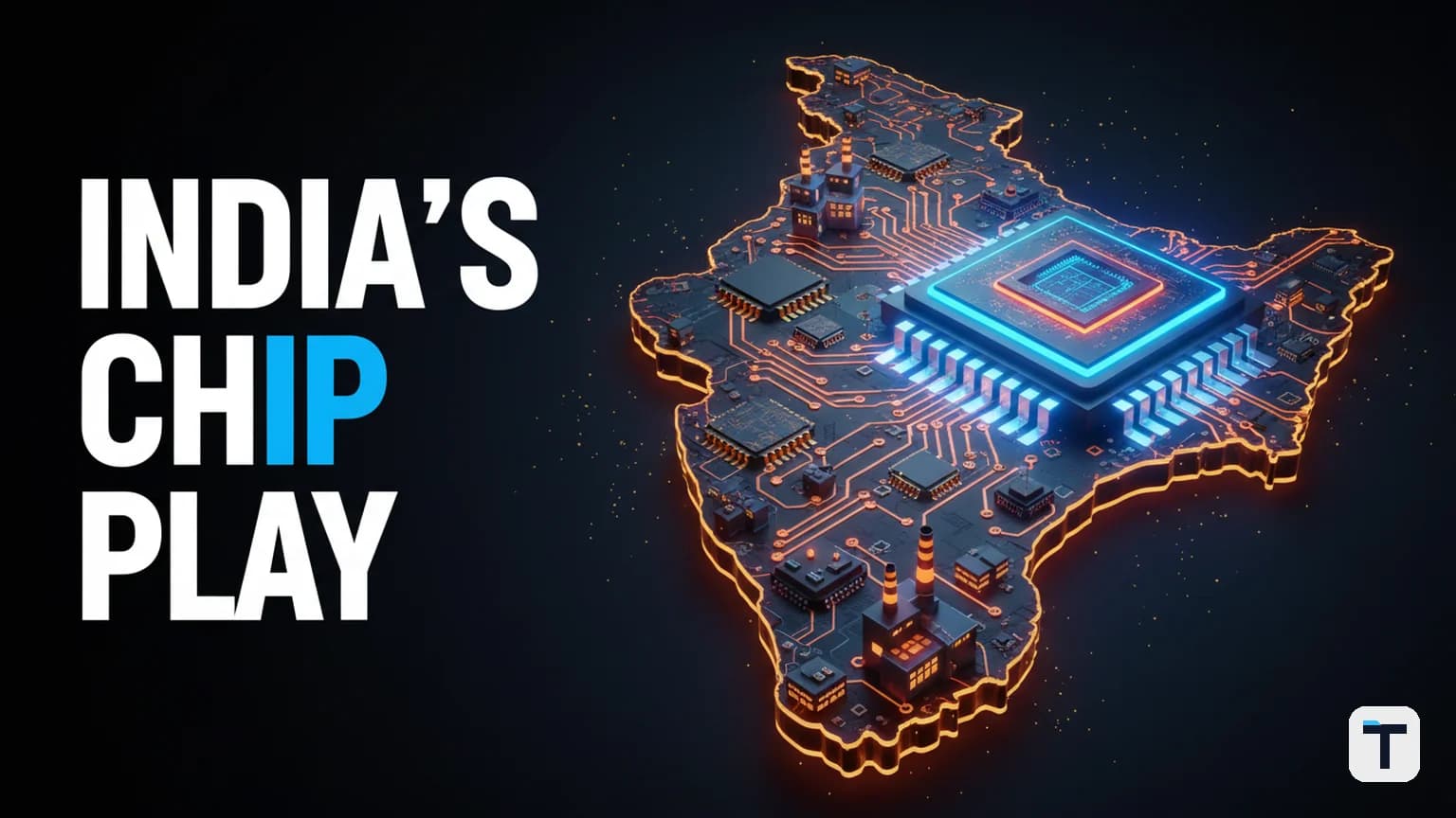

India's central government has approved two new Electronics Manufacturing Clusters (EMCs) in Tamil Nadu with a combined project cost of Rs 1,012 crore, extending the state's existing electronics corridor into two new industrial zones. The approval, announced by Union Minister Ashwini Vaishnaw on July 22, 2026, allocates Rs 587.47 crore to a 474.3-acre cluster at Manallur and Rs 424.55 crore to a 379.3-acre cluster at Pillapaikkam. Both fall under the Modified Electronics Manufacturing Clusters (EMC 2.0) scheme and arrive just one week after the Cabinet cleared Semicon 2.0, a Rs 1,27,500 crore push to deepen India's semiconductor ecosystem across six strategic pillars.
Last verified: July 29, 2026
- Two EMCs approved: Manallur (474.3 acres, Rs 587.47 crore) and Pillapaikkam (379.3 acres, Rs 424.55 crore)
- Total investment: Rs 1,012.02 crore, sanctioned under MeitY's EMC 2.0 scheme
- Tamil Nadu posted 13.7 percent export growth in FY26 — the fastest of any Indian state
- Kanchipuram district is India's second-largest merchandise exporting district ($26.4 billion), behind only Jamnagar
- Semicon 2.0 (Rs 1,27,500 crore) was approved by Cabinet on July 15, 2026, with six pillars covering the full chip value chain
What Are Electronics Manufacturing Clusters and Why Does the EMC 2.0 Scheme Exist?
Electronics Manufacturing Clusters are government-funded industrial zones built specifically for electronics and semiconductor companies. Instead of each company negotiating land, power, water, and logistics separately, the cluster model bundles all of that infrastructure up front — plug-and-play plots, ready-built factory sheds, common facility centres, and logistics connectivity configured for electronics manufacturing needs.
The EMC 2.0 scheme was notified by the Ministry of Electronics and Information Technology (MeitY) on April 1, 2020, with a total budgetary support of Rs 3,762 crore and an implementation period running through March 2028. STPI (Software Technology Parks of India) serves as the Project Management Agency. Applications were accepted through March 2024, but fund disbursement for approved projects continues until 2028.
The scheme's stated objective is to create "a comprehensive supply chain ecosystem for strengthening the electronics manufacturing base" — attracting anchor units along with their entire supplier network rather than building standalone factories and hoping suppliers follow.
Where Are the Two New Tamil Nadu Clusters Located?
The two new clusters sit in Tamil Nadu but draw their strategic logic from the existing Kanchipuram electronics corridor. According to the PIB press release dated July 22, 2026, the first cluster covers 474.3 acres at Manallur with a project cost of Rs 587.47 crore, and the second covers 379.3 acres at Pillapaikkam with a project cost of Rs 424.55 crore.
Kanchipuram district, which already hosts 38 electronics manufacturing plants — the most of any district in Tamil Nadu — recorded $26.4 billion in merchandise exports in FY26, making it India's second-largest exporting district after Jamnagar in Gujarat ($36.6 billion). The district houses Foxconn and Pegatron smartphone manufacturing operations, which have driven Tamil Nadu's electronics exports to roughly $20 billion, accounting for 42 percent of India's total electronics exports.
The new clusters extend that existing corridor rather than starting a new manufacturing base from zero. This geographic continuity matters: component makers, packaging units, testing facilities, and logistics partners are already operating in the region.
How Does the Semicon 2.0 Programme Connect to These Clusters?
The Cabinet approved Semicon 2.0 on July 15, 2026, with a total budget outlay of Rs 1,27,500 crore — nearly doubling the Rs 76,000 crore allocated under Semicon 1.0 in December 2021. The programme is structured around six strategic pillars, each targeting a different layer of the semiconductor value chain:
| Pillar | Focus | Key Detail |
|---|---|---|
| 1. Design | Indigenous chip IP | 105 startups already developing chips; DLI scheme supports seed money + EDA tools |
| 2. Machines & Materials | Equipment, chemicals, gases | Incentivises domestic production of photomasks, ultra-pure gases, specialty chemicals |
| 3. More fabs | Silicon, compound, discrete, display | 40 percent capex support for CMOS silicon fabs; 35 percent for other fab types |
| 4. ATMP/OSAT | Assembly, testing, packaging | 35 percent capex for advanced packaging; 25 percent for conventional packaging |
| 5. R&D | Advanced process nodes | Targets 2nm/3nm nodes beyond current 28nm-65nm range |
| 6. Talent | Workforce training | 315 institutes nationwide (61 in Tamil Nadu); Rs 1,000 crore for industry-led research centres |
The EMC clusters are the physical infrastructure that hosts the facilities Semicon 2.0 incentivises — particularly the fabs, ATMP, and OSAT capacity targeted by Pillars 3 and 4. A semiconductor fabrication plant or packaging facility needs ready-to-use industrial land with power, water, and logistics configured to semiconductor-grade specifications. That is exactly what the EMC 2.0 scheme funds.
What Does a Company Get When an EMC Is Built?
Once an electronics manufacturing cluster becomes operational, companies receive ready infrastructure that compresses the timeline between deciding to build a factory and actually manufacturing products. Specifically:
- Plug-and-play industrial plots — land already zoned, levelled, and utility-connected, sized for electronics manufacturing rather than generic industry.
- Ready Built Factory (RBF) sheds — pre-constructed factory buildings that companies can occupy immediately, eliminating 12-18 months of construction.
- Common Facility Centres (CFCs) — shared testing labs, prototyping facilities, and quality certification infrastructure that individual companies would otherwise build independently.
- Power, water, and logistics connectivity — substations, water treatment, road and port access designed for electronics supply chain scale.
- Pre-approved regulatory clearances — environmental and industrial permits handled at the cluster level rather than company-by-company.
The economic logic: a single electronics plant needs suppliers nearby — component makers, packaging units, testing facilities, logistics partners. The cluster model tries to attract that entire ecosystem into one zone at once, rather than hoping suppliers eventually follow one anchor factory over years. That is the same model that grew Kanchipuram's Foxconn and Pegatron operations into India's electronics export engine.
How Fast Is Tamil Nadu's Electronics Sector Growing?
What is Tamil Nadu's export growth rate?
Tamil Nadu registered 13.7 percent year-on-year growth in merchandise exports in FY26, the highest of any Indian state, reaching $59.3 billion. Electronics exports accounted for roughly $20 billion of that total, up 36 percent year-on-year, giving Tamil Nadu a 42 percent share of India's total electronics exports.
How many electronics manufacturing plants are in Tamil Nadu?
According to the PIB data, Tamil Nadu hosts 67 government-supported electronics manufacturing plants across nine districts:
| District | Plants |
|---|---|
| Kanchipuram | 38 |
| Krishnagiri | 8 |
| Chennai | 6 |
| Tiruvallur | 6 |
| Chengalpattu | 4 |
| Thoothukudi | 2 |
| Coimbatore | 1 |
| Tirunelveli | 1 |
| Vellore | 1 |
How much has India's electronics manufacturing grown overall?
India's electronics goods production grew from approximately Rs 1.9 lakh crore in 2014-15 to Rs 13.11 lakh crore in 2025-26 — a sevenfold increase. Electronics exports grew 11x, from Rs 38,000 crore to Rs 4.24 lakh crore. Mobile phone production alone grew 33x, from Rs 18,000 crore to Rs 6.27 lakh crore, making mobile phones India's single largest exported item. By February 2025, 99.2 percent of mobile phones sold in India were manufactured domestically.
What Other Semiconductor Investments Is Tamil Nadu Attracting?
Tamil Nadu's semiconductor momentum extends beyond the two EMC approvals. Seoul Semiconductor, one of the world's largest LED and optoelectronics manufacturers, is in talks with the Tamil Nadu state government (along with Karnataka and Gujarat) about establishing a manufacturing plant in India and may seek incentives from the Semicon 2.0 programme.
At the state level, Tamil Nadu has its own Semiconductor Mission 2030, announced in the State Budget 2025-26. The mission partners with IIT Madras to launch a Centre for Advanced Semiconductor Technologies at the Central Polytechnic Campus in Chennai, housing India's first in-situ semiconductor fab processing facility. The state government provided an initial seed grant of Rs 100 crore, with plans to train over 4,500 professionals through short-term skilling programmes.
Under the central Design-Linked Incentive (DLI) scheme, seven Tamil Nadu companies have already received support: Aheesa Digital Innovations, Mindgrove Technologies, InCore Semiconductors, and MBit Wireless (all Chennai-based, receiving grants plus EDA tools), plus Struent Semiconductors and PRSsemicon Technologies (Chennai) and Sicrest Semiconductors (Coimbatore) receiving EDA tool support.
How Does the Cluster Model Compare to Standalone Factory Incentives?
| Factor | Standalone Factory | EMC Cluster Model |
|---|---|---|
| Land acquisition | Company negotiates individually | Pre-zoned, pre-levelled plots |
| Infrastructure | Company builds power, water, roads | Government provides ready infrastructure |
| Supplier ecosystem | Suppliers follow over years | Suppliers attracted simultaneously |
| Time to production | 18-36 months | 6-12 months with RBF sheds |
| Common facilities | Each company builds own labs | Shared CFCs reduce costs |
| Regulatory permits | Company-by-company | Cluster-level pre-approval |
The comparison explains why India shifted from the PLI-for-large-scale-electronics model (which incentivised individual factories) toward the EMC cluster model for semiconductor infrastructure. A fab or ATMP facility cannot function without a local supply of specialty chemicals, clean-room construction expertise, testing partners, and precision logistics. The cluster model front-loads that ecosystem rather than waiting for it to assemble organically.
What This Means for You
If you are building or sourcing hardware in India, the Tamil Nadu cluster approvals signal three things:
- For electronics manufacturers: Manallur and Pillapaikkam will offer ready infrastructure within the next 12-24 months. If you are evaluating Tamil Nadu for an electronics or semiconductor facility, the EMC framework removes the infrastructure negotiation bottleneck.
- For supply chain managers: The cluster model means component suppliers, testing labs, and packaging partners will co-locate. If your current supplier base is concentrated in China or Vietnam, Tamil Nadu's cluster development offers a de-risking path.
- For investors and analysts: The Rs 1,012 crore cluster investment is infrastructure seed capital — the facility-building layer beneath Semicon 2.0's Rs 1,27,500 crore incentive programme. Watch for anchor tenant announcements at both sites as the leading indicator of ecosystem formation.
If you are evaluating AI infrastructure and compute build-outs that depend on chip supply chains, understanding where the physical semiconductor ecosystem is forming matters — OpenAI's $750 billion infrastructure plan and the Chinese AI model landscape both intersect with the global chip supply that India is building domestic capacity to serve.
FAQ
Q: What is the EMC 2.0 scheme? A: The Modified Electronics Manufacturing Clusters (EMC 2.0) scheme is a MeitY programme notified on April 1, 2020, with a budget of Rs 3,762 crore. It funds ready-to-use industrial infrastructure — plug-and-play plots, factory sheds, common facility centres — specifically configured for electronics and semiconductor manufacturing. Fund disbursement runs through March 2028.
Q: How much investment was approved for the Tamil Nadu clusters? A: The Centre approved two clusters with a combined project cost of Rs 1,012.02 crore — Rs 587.47 crore for the Manallur cluster (474.3 acres) and Rs 424.55 crore for the Pillapaikkam cluster (379.3 acres), as per the PIB press release dated July 22, 2026.
Q: What is Semicon 2.0 and how much is it worth? A: Semicon 2.0 is the second phase of India's Semiconductor Mission, approved by the Cabinet on July 15, 2026, with a total outlay of Rs 1,27,500 crore. It builds on Semicon 1.0 (Rs 76,000 crore, approved December 2021) and covers six pillars: design, machines and materials, fabs, ATMP/OSAT, R&D, and talent development.
Q: Why is Tamil Nadu receiving these clusters? A: Tamil Nadu posted the fastest export growth of any Indian state in FY26 at 13.7 percent, reaching $59.3 billion. Kanchipuram district — already home to Foxconn and Pegatron — is India's second-largest merchandise exporting district at $26.4 billion. The new clusters extend this proven electronics corridor rather than building a new one from scratch.
Q: What is the difference between a semiconductor fab and an ATMP/OSAT facility? A: A fab (fabrication plant) etches integrated circuits onto silicon wafers — the most capital-intensive layer of chip manufacturing. ATMP (Assembly, Testing, Marking, and Packaging) and OSAT (Outsourced Semiconductor Assembly and Test) are the "back-end" steps where finished wafers are cut, packaged, and tested. India has gained early commercial traction in ATMP/OSAT under Semicon 1.0; Semicon 2.0 deepens both.
Q: How many semiconductor professionals does India need? A: India faces a shortage of approximately 300,000 semiconductor professionals, according to industry reports cited in the Cyril Amarchand Mangaldas analysis of Semicon 2.0. The programme addresses this through 315 institutes nationwide (61 in Tamil Nadu) and Rs 1,000 crore allocated for industry-led research and training centres in FY 2026-27.
Discussion
0 comments