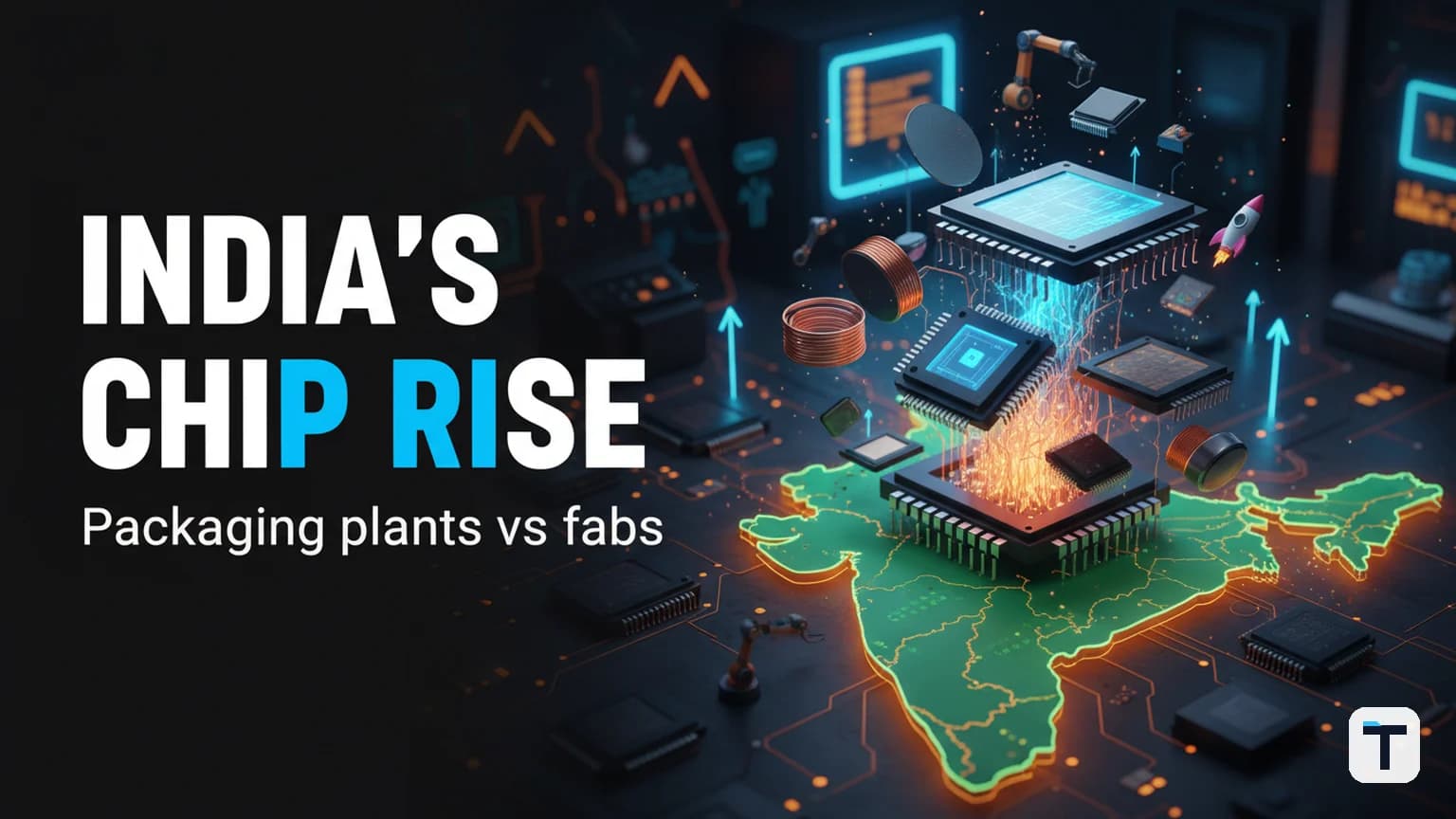

Verdict: The ASIP Technologies facility at Tarluvada, Visakhapatnam — inaugurated virtually by Prime Minister Narendra Modi on 1 August 2026 — is a genuine milestone for India's semiconductor build-out. It is the first India Semiconductor Mission (ISM)-approved OSAT plant in Andhra Pradesh and South India, with a planned ₹2,500 crore investment and 96-million-chips-per-year packaging capacity. But here's the honest part most coverage skips: it will not fabricate a single transistor. India is winning at outsourced semiconductor assembly and test (OSAT) far faster than at wafer fabrication, because packaging is a real but lower rung on the chip value chain. That's still progress — and it's the rung India can actually climb right now.
Last verified: 2026-08-03 · Verdict: ASIP's Vizag OSAT is real, India-first, and reduces import dependence — but it packages chips, doesn't manufacture them. India has 4+ operational OSATs and zero commercial fabs as of mid-2026. Punctuation matters here: OSAT ≠ fab.
What Is the ASIP Technologies Plant in Andhra Pradesh?
The ASIP Technologies facility is a 30-acre Outsourced Semiconductor Assembly and Test (OSAT) plant in Tarluvada village, Visakhapatnam, Andhra Pradesh, with a planned total investment of ₹2,500 crore and an initial outlay of over ₹460 crore already committed (Manufacturing Today India, 1 Aug 2026). ASIP Managing Director and CEO Venkata Simhadri leads the project, partnered with South Korea's APACT Co. as technology provider — APACT's CEO and President is Seong Dong Lee (Economic Times, 31 Jul 2026).
Key numbers verified against primary coverage:
- Capacity: 96 million chips per year at full scale
- Initial investment: ₹460+ crore, with plans for an additional ₹2,000 crore as demand grows (ET Electro)
- Employment: 1,000+ direct skilled jobs and ~1,600 indirect jobs
- Target markets: AI, high-performance computing, data centres, and high-speed communications
- Initial tech: Wire bond and flip-chip ball grid array (FC-BGA) packaging — established, decades-old processes
- Advanced tech: 2.5D and 3D packaging scheduled to arrive within 2–3 years
Amitesh Kumar Sinha, CEO of the India Semiconductor Mission, called the project "a very important contribution to India's semiconductor ambitions." Andhra Pradesh Chief Minister N. Chandrababu Naidu joined virtually.
What Does an OSAT Actually Do — and What Doesn't It Do?
An OSAT — Outsourced Semiconductor Assembly and Test — takes finished silicon wafers fabricated elsewhere and turns them into shippable packaged chips: dicing, bonding, encapsulation, marking, and final electrical test (Wevolver, OSAT primer). It does not manufacture the wafer. It does not etch transistors. It does not draw circuit patterns with lithography. By industry convention, that upstream work — front-end wafer fabrication — is what "manufacturing a chip" usually means.
This matters because ASIP's 96-million-chip capacity is measured in packaged chips, not fabricated dies. The dies arrive from foundries like TSMC, Samsung, or (eventually) Tata-PSMC's Dholera fab. ASIP then packages those dies for customers in automotive, computing, and consumer electronics. India's supply-chain dependency on imported dies does not shrink because of ASIP — ASIP only changes where the final assembly happens.
Packaging and test together typically account for roughly 25–40% of a chip's total assembled cost, with the share varying widely by package type and node. For advanced AI chips using TSMC CoWoS-S 2.5D integration, the packaging layer alone costs ~$70 per unit and CoWoS-S supply is currently constrained by 40–50% demand-supply gap with 40–52 week lead times (Silicon Analysts, July 2026). OSAT is genuinely valuable work — but it isn't fabrication, and the distinction matters for any honest analysis of India's chip progress.
How Does ASIP Vizag Compare to India's Other Semiconductor Plants?
The clearest way to read India's semiconductor story is the OSAT-vs-fab split. As of mid-2026, India has multiple OSAT/ATMP plants operational or under construction, but zero commercial wafer fabs producing logic chips.
| Plant | Location | Type | Investment | Status | First Output |
|---|---|---|---|---|---|
| Micron ATMP | Sanand, Gujarat | ATMP (memory packaging) | ~₹2,750 crore | Operational since Feb 2026 | Commenced 28 Feb 2026 |
| Kaynes Semicon OSAT | Sanand, Gujarat | OSAT (auto/industrial) | ₹3,307 crore | Operational since Mar 2026 | 31 Mar 2026 |
| CG Power–Renesas–STARS | Sanand, Gujarat | OSAT | Under execution | Sanctioned | TBD |
| ASIP–APACT | Tarluvada, Visakhapatnam, AP | OSAT (AI/HPC packaging) | ₹2,500 crore | Foundation stone laid 1 Aug 2026 | 2.5–3 years to advanced packaging |
| HCL–Foxconn (India Chip) | Jewar, Uttar Pradesh | OSAT | Sanctioned | Groundbreaking Feb 2026 | TBD |
| Tata Semicon ATMP | Jagiroad, Morigaon, Assam | ATMP | ~₹27,000 crore | Under execution | TBD |
| Tata Electronics–PSMC Fab | Dholera, Gujarat | Front-end fab (28–110nm, 300mm) | ₹91,000 crore | Under construction | First silicon ~late 2026; full ramp ~2028 |
Sources: India Semiconductor Mission (ism.gov.in), Anantam IAS plant tracker, Fidus Dholera project tracker.
The takeaway from the table: India is assembling and packaging chips at scale today. India is not fabricating chips at commercial scale, and the only project on track to change that — the Tata-PSMC Dholera fab — is targeted for first process-qualification wafers in late 2026 and full production around 2028 (Fidus tracker, confirmed by Union Minister Ashwini Vaishnaw). And even Dholera starts at 28nm–110nm, decades behind TSMC's 2nm frontier (India Today, 17 Jul 2026 — reports suggest initial output at 90nm, with 28nm to follow).
Why Is India Building OSATs So Much Faster Than Fabs?
Because OSATs are an order of magnitude simpler to set up. A fab requires mastery of thousands of process steps — deposition, lithography, etching, metrology — and infrastructure most countries don't have: hundreds of millions of litres of ultrapure water per day, uninterrupted high-grade power, and a deep ecosystem of equipment vendors and process engineers. An OSAT, by contrast, works with already-fabricated wafers and demands a different (lower) skills mix: process engineering for die-attach and wire bonding, equipment maintenance, quality control, and supply chain management.
The Indian government recognised this gap explicitly when it designed the Semicon India Programme — applications for OSAT and ATMP subsidies are required to have a foreign technology partner, precisely because domestic expertise is thin (DIGITIMES interview with Venkata Simhadri, March 2024). ASIP-APACT follows that template: ASIP supplies the local facility, APACT supplies the established process know-how from its base in Anseong-Si, South Korea, where it began as an SK Hynix joint venture spin-off in 2002 (Blackridge Research). ASIP has also partnered with IIT Hyderabad on R&D.
The pattern isn't unique to ASIP. Tata's fab tech partner is Taiwan's PSMC; Micron brought its own ATMP playbook to Sanand; the CG Power OSAT JV brings Renesas and STARS Microelectronics into the mix. India is compressing the learning curve by importing the part of the process it can't yet do alone.
What Does This Mean for India's Self-Reliance in Semiconductors?
The honest answer: less than the headlines suggest, but more than nothing. India imported about $6.1 billion in semiconductor devices in 2024 (The Observatory of Economic Complexity), and integrated-circuit imports under HS Code 85423100 reached approximately $17.78 billion in 2025 (NBD Data, Jan 2026). China supplied roughly $4.42 billion of India's 2024 semiconductor imports.
An OSAT plant reduces India's dependence on imported packaged chips — it does not reduce dependence on imported bare dies. The value chain ASIP plugs into looks like this:
- Bare wafers are still fabricated overseas (or eventually at Tata-PSMC Dholera — but not for 2–3+ years at commercial scale, and only at mature nodes).
- ASIP performs the back-end — assembly, packaging, test — and ships a finished chip to the customer.
- The packaged chip replaces an otherwise-imported finished packaged product.
That substitution is real value: it captures a meaningful chunk of the onshore supply chain, builds domestic process-engineering capability, and creates the kind of cluster effects that attracted the 105 chip-design startups and 68,000 EDA-trained students India is now incubating under Semicon 2.0 (Business Today, 15 Jul 2026). But declaring "India's chip dream" realised because of one OSAT would be like celebrating a car-assembly plant as proof you can forge engine blocks.
What Is Semicon 2.0 and Why Does It Change the Picture?
On 15 July 2026, the Union Cabinet approved Semicon 2.0 — a ₹1,27,500 crore ($15.3 billion) programme expanding India's semiconductor ambitions across six pillars: design, equipment and materials, additional fabs, ATMP/OSAT strengthening, R&D, and talent development (PMO India press release; India Today, 15 Jul 2026). Semicon 1.0 had a ₹76,000 crore outlay and approved 12 manufacturing units; Semicon 2.0 nearly doubles the budget and broadens scope to the upstream end India has so far skipped — equipment, materials, and design IP.
For a piece of large-industry context — the kind of state-vs-state industrial contest that determines whether Vizag becomes a serious node — you can read our analysis of Chennai's GCC boom and India's $150B tech-hub race. The ASIP plant is the same competitive dynamic in semiconductors: Andhra Pradesh offered land and incentives, Vizag brings a deep-water port and existing tech-talent base, and the state is now on the semiconductor map where it had no presence a year ago. For a related angle on what the state was trying to do on the AI compute side — and the update that conspicuously went missing — see Andhra Pradesh's NVIDIA deal: why the update is missing in 2026.
What This Means for You
If you're a small business or system integrator in India buying components: ASIP's plant doesn't change your bill of materials tomorrow — first commercial output is still years away — but the OSAT cluster as a whole (Micron, Kaynes, ASIP, CG Power) is starting to offer locally-packaged parts to OEMs. If you're sourcing for AI/HPC workloads, ASIP specifically targets your segment.
If you're an engineer or job-seeker: 1,000 direct and ~1,600 indirect jobs is real, and ASIP-APACT's partnership includes a worker-training exchange with Korea. The skill mix is process engineering, equipment maintenance, yield analysis, and supply-chain — not chip design. For the design-track jobs being created by Semicon 2.0's design pillar, see our teardown of India's enterprise AI skills gold rush — AICTE, vendor deals, and the courses being launched.
If you're an investor or policymaker: the headline risk is hype presenting packaging as fabrication. India currently has zero commercial wafer fabs and the realistic near-term ceiling of any OSAT is to substitute for imported packaged parts; until Dholera produces commercial silicon (~2028), every "made in India" chip narrative that uses OSAT output as evidence hides a fundamental die import dependency. Read our India sovereign AI strategy piece for why chasing the frontier is the wrong frame, and why the AI chip bottleneck reaches into models like Kimi K4 — the upstream fab problem isn't abstract; it constrains what AI labs can ship.
FAQ
Q: Is the ASIP Vizag plant India's first semiconductor fab?
A: No. The ASIP facility is an OSAT — Outsourced Semiconductor Assembly and Test — plant. It packages and tests chips that were fabricated elsewhere. India's first commercial front-end wafer fab is the Tata Electronics-PSMC Dholera facility, targeted for first silicon in late 2026 and full ramp around 2028.
Q: What is the difference between OSAT and a semiconductor fab?
A: A fab fabricates chips on silicon wafers using lithography and process chemistry — it etches transistors. An OSAT takes finished wafers and performs back-end assembly: die bonding, packaging, marking, and final test. OSAT is genuinely valuable work, but it does not create the chip's circuit.
Q: Who is the technology partner for ASIP's Vizag plant?
A: APACT Co., a South Korea–based OSAT founded in 2002 originally as an SK Hynix joint venture spin-off, headquartered in Anseong-Si. APACT's CEO is Seong Dong Lee. ASIP Technologies is headquartered in Hyderabad; the Tarluvada facility is its first manufacturing plant in Andhra Pradesh.
Q: How many chips will the ASIP plant produce, and when?
A: Annual capacity is 96 million chips at full scale. Initial production uses wire-bond and flip-chip ball grid array (FC-BGA) packaging — established technologies. Advanced 2.5D and 3D packaging — the kind that supports AI accelerators and high-bandwidth memory integration — is planned within 2–3 years of groundbreaking.
Q: How does ASIP fit into India's broader semiconductor strategy?
A: ASIP is the fourth major OSAT/ATMP project to break ground or commence operations in India in 2026, after Micron's Sanand ATMP (Feb 2026), Kaynes Semicon's Sanand OSAT (Mar 2026), and the CG Power–Renesas–STARS OSAT at Sanand. India is building OSAT capacity far faster than wafer fab capacity, because packaging is technically simpler and accepts foreign technology partners more readily. ASIP is the first such plant in Andhra Pradesh and South India.
Q: Does the ASIP plant reduce India's dependence on imported chips?
A: Partially. It substitutes for imported packaged chips by performing the assembly step onshore. It does not, however, eliminate dependence on imported bare silicon dies — those continue to be fabricated overseas until Tata-PSMC Dholera reaches commercial production around 2028. India's semiconductor imports reached approximately $17.78 billion in integrated circuits alone in 2025.
Q: What is Semicon 2.0 and how does it affect ASIP?
A: Semicon 2.0 is the ₹1,27,500 crore next phase of India's semiconductor mission, approved by the Union Cabinet on 15 July 2026. It expands scope to six pillars — design, equipment and materials, additional fabs, ATMP/OSAT strengthening, R&D, and talent — broadening beyond the OSAT-heavy Semicon 1.0 portfolio that ASIP was approved under. ASIP itself was sanctioned under ISM 1.0; future expansion could attract Semicon 2.0 incentives for advanced 2.5D/3D packaging.
Discussion
0 comments