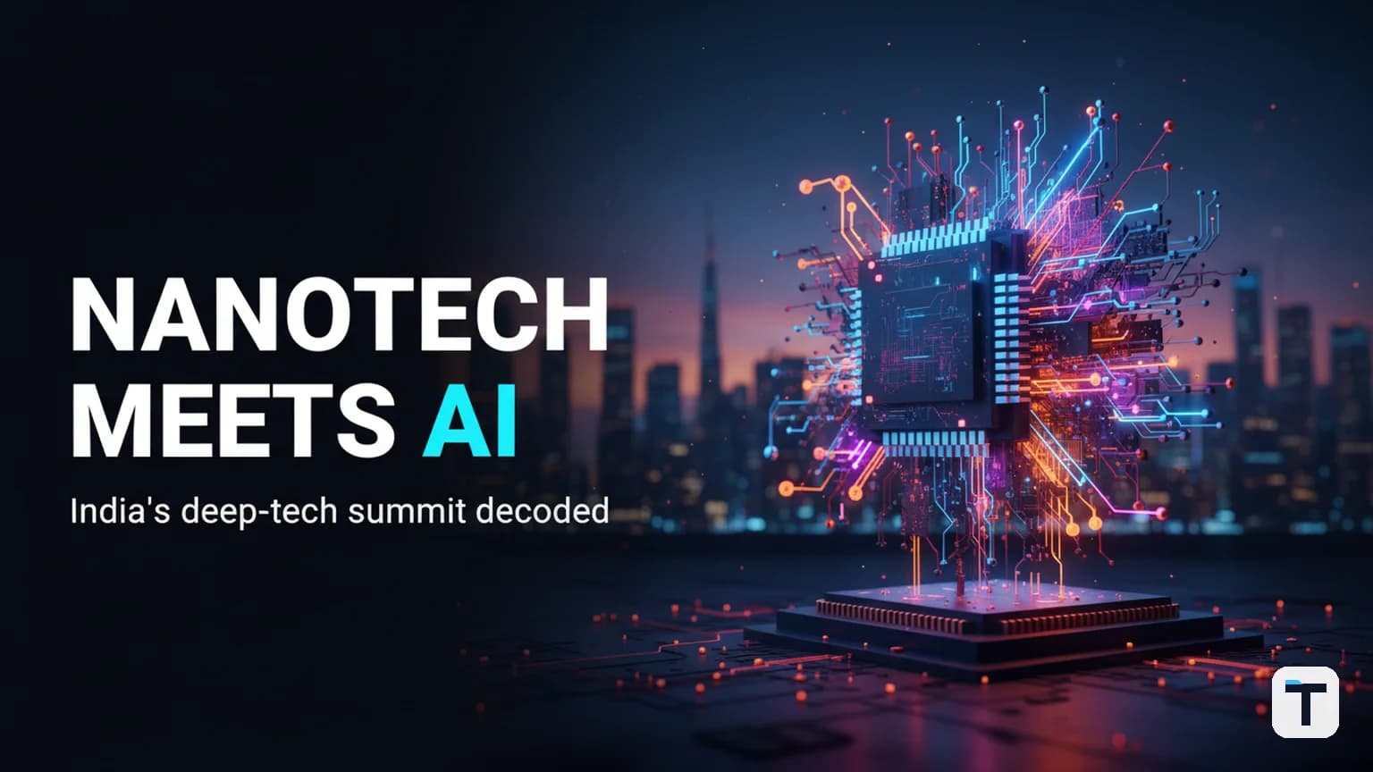

Verdict: India's 14th Bengaluru INDIA NANO summit (3–5 August 2026) confirmed that nanotechnology and AI have stopped being separate disciplines — they now need each other to cross the lab-to-market gap. The real story is not the conference itself but the commercialization infrastructure behind it: the Centre for Nano Science and Engineering (CeNSE) at IISc, the ₹76,000 crore India Semiconductor Mission, and Karnataka's "government as first customer" deep-tech procurement policy. For builders and researchers, the takeaway is that nanotech in India is no longer just papers and posters — it is becoming chips, sensors, and startups, with AI as the accelerator.
Last verified: 2026-08-04
- India Nano 2026 (14th edition) ran 3–5 August at The LaLiT, Bengaluru, themed "Nanotech's Next Frontier: AI & Beyond — Conceive, Converge, Commercialise."
- Three technical tracks: Nano in Semiconductors, Nano in Agriculture & Health, Nano in Energy & Environment.
- India's semiconductor market was valued at ~USD 47.5–59.8 billion in 2025 (estimates vary by source), projected to grow at 12–15% CAGR through 2034.
- The India Semiconductor Mission has a ₹76,000 crore (~USD 10 billion) outlay, with six approved projects totalling over ₹1.6 lakh crore in committed investment.
- Karnataka's Startup Policy 2025–30 commits ₹570 crore and includes a "Government First" initiative — the state buys from its own deep-tech startups.
What is the India Nano summit and why does it matter?
India Nano is India's flagship international nanotechnology conference and exhibition, organized by the Department of Science & Technology, Government of Karnataka, under the guidance of the Vision Group on Nanotechnology chaired by Prof. C.N.R. Rao, FRS, of JNCASR (bengaluruindianano.in). The 2026 edition — the 14th — ran from 3 to 5 August at The LaLiT in Bengaluru, drawing over 80 speakers, 1,000+ delegates, 50 exhibitors, and participants from more than 10 countries (Daily Excelsior, 25 Jul 2026).
What makes this edition different is the explicit theme: "Nanotech's Next Frontier: AI & Beyond — Conceive, Converge, Commercialise." The framing is deliberate. Nanotechnology has spent two decades producing world-class research from Indian institutes — IISc, IITs, JNCASR, CSIR-NCL — but the persistent gap has been turning that research into products people can buy. The 2026 event is built around the idea that AI is now the tool that can close that gap, from AI-driven materials discovery to AI-optimized nanoscale fabrication.
How does nanotechnology connect to India's semiconductor push?
The connection is direct and structural. Every modern semiconductor is a nanotechnology product — today's chips are fabricated at process nodes of 28 nm down to 3 nm, features measured in nanometres. The India Semiconductor Mission (ISM), launched by the Union Cabinet on 15 December 2021 with a ₹76,000 crore (~USD 10 billion) outlay, is the government's flagship push to build domestic chip fabrication, packaging, and design capability (PIB, 15 Dec 2021; ism.gov.in).
By mid-2026, the ISM has approved six semiconductor projects with a combined committed investment of over ₹1.6 lakh crore (~USD 19 billion):
| Project | Location | Investment | Type |
|---|---|---|---|
| Tata-PSMC fab | Dholera, Gujarat | ₹91,000 crore | 28 nm wafer fabrication |
| Micron ATMP | Sanand, Gujarat | $2.75 billion | Assembly, testing, packaging |
| CG Power-Renesas-Stars | Sanand, Gujarat | ₹7,600 crore | OSAT (power-management ICs) |
| Tata Electronics OSAT | Jagiroad, Assam | ₹27,000 crore | OSAT/ATMP |
| Kaynes Semicon | Sanand, Gujarat | ₹3,300 crore | ATMP |
| HCL-Foxconn | Jewar, Uttar Pradesh | ₹3,706 crore | Display-driver IC fab |
Sources: PIB, ism.gov.in; aggregate investment per anantamias.com analysis, May 2026
The India Nano 2026 "Nano in Semiconductors" track — covering advanced materials, nanoscale fabrication, and innovative chip architectures — maps directly onto the ISM's needs. The summit's pre-conference tutorial on advanced semiconductor manufacturing (fabrication, packaging, lithography, materials) reflects how the event has pivoted from pure academic nanoscience toward the industrial pipeline India is actually building.
Where is India's nanotech research actually happening?
The research backbone is the Centre for Nano Science and Engineering (CeNSE) at the Indian Institute of Science (IISc), Bengaluru. CeNSE operates a national shared facility where researchers, startups, and industry users can fabricate, characterize, package, and test semiconductor devices — moving from plain wafers to packaged components on a single campus (EE Times; IISc).
CeNSE is not a standard university lab. It functions as a national facility: its Industry Affiliate Program has attracted partners like Applied Materials India, the U.S. materials engineering leader, which joined to explore advanced materials applications and bring solutions "from Lab to Fab" (Express Computer, 23 Mar 2021). This is the kind of infrastructure that makes the "commercialize" in the summit's theme credible — researchers and startups have access to fabrication and testing equipment that would otherwise require millions in capital to access.
CeNSE also supports India's broader deep-tech ecosystem through the Indian Nanoelectronics User Program (INUP), a government-backed program jointly run by IIT Bombay and IISc Bengaluru that makes nanoelectronics research facilities accessible to researchers across the country.
Who are the key speakers at India Nano 2026 and what do they signal?
The speaker lineup reveals who India is bringing in to bridge the lab-to-market gap. The confirmed speakers include (bengaluruindianano.in):
- Prof. Umesh V. Waghmare — Secretary, Department of Science & Technology, Government of India. As the central government's top science official on stage, he represents the national policy layer.
- Prof. Chennupati Jagadish — Distinguished Professor (Emeritus), Research School of Physics, Australian National University. A Fellow of the Royal Society (elected 2025) and Companion of the Order of Australia (2016), Jagadish is one of the world's most cited nanotechnology researchers, with expertise in compound semiconductor optoelectronics and nanowire devices (ANU profile).
- Prof. Akshay Rao — Professor of Physics, Cavendish Laboratory, University of Cambridge. Rao's research focuses on energy and quantum materials — developing new technologies to enhance the efficiency of silicon solar cells and new tools for battery research. He is co-founder of Cambridge Photon Technology and Illumion (Cambridge Physics profile).
- Dr. B.L.V. Prasad — Chief Scientist, Physical/Materials Chemistry Division, CSIR-National Chemical Laboratory. Represents India's CSIR lab network, which bridges fundamental chemistry and industrial materials.
- Dr. Subra Herle — CTO, Elevated Materials, USA. Industry-side perspective on advanced materials commercialization.
- Prof. Radha Boya — Department of Physics and Astronomy, University of Manchester, UK (2D materials and nanofluidics).
The signal is clear: this is not a purely domestic academic conference. It is pulling in global researchers who have themselves crossed the commercialization bridge — people who have founded companies, hold patents, and have shipped products.
What is Karnataka's "first customer" deep-tech policy?
Karnataka's Home Minister Priyank Kharge — who also holds the Electronics, IT, Biotechnology, and e-Governance portfolios — has framed the event around one idea: research only matters once it becomes something people can buy. He has called Karnataka "India's nanotech capital," though this framing comes from the state organizing the event rather than from an independent ranking (BusinessWorld).
The substance behind the branding is real, however. Karnataka unveiled its Startup Policy 2025–30 in January 2026, committing over ₹570 crore to position the state as a global hub for deep-tech and science-led entrepreneurship (The Hindu BusinessLine, 17 Jan 2026). The policy targets the creation of 25,000 startups by 2030, with at least 10,000 expected from clusters outside Bengaluru.
The standout mechanism is the "Government First" initiative, which allows eligible startups to pilot and sell solutions directly to Karnataka government departments as their first customer (Daijiworld; Deccan Herald). This is designed to shorten the go-to-market cycle for early-stage deep-tech ventures — and nanotech startups pitching at NanoSparX, the summit's startup pitch competition, are exactly the intended beneficiaries.
How is AI accelerating nanotechnology commercialization?
The summit's most pointed talk title — "Enabling AI with AI" — signals something broader than a single session. Here is the actual convergence, based on what the event's tracks and tutorials cover:
AI for materials discovery. The pre-conference tutorial on "AI & ML for Sciences and Engineering" covers how machine learning accelerates data analysis, simulation, design optimization, and discovery in nanoscience. Instead of trial-and-error in a wet lab, researchers use AI to predict which nanomaterial structures will have the properties they need — compressing what used to take years into weeks.
AI-driven nanoscale fabrication. The semiconductor track covers how AI is being used to optimize lithography, process control, and yield management in chip manufacturing. This is not theoretical — Applied Materials, the Gold Partner of India Nano 2026, is the world's largest supplier of semiconductor manufacturing equipment, and its products increasingly embed AI for process optimization.
Nanotech enabling AI hardware. This is the reverse direction — nanotechnology is what makes advanced AI chips possible. The sub-2 nm process nodes that NVIDIA, AMD, and Apple rely on are nanofabrication achievements. India's push into 28 nm at the Tata-PSMC Dholera fab is the entry point to this value chain.
Nanotech in healthcare with AI diagnostics. The Agriculture & Health track covers precision delivery systems and smart diagnostics. AI-powered diagnostic tools that use nanoscale sensors for point-of-care testing are a fast-growing segment where India's strengths in both AI and frugal engineering converge.
The big picture: India has a strong research base in nanotechnology, a rapidly growing AI ecosystem, and a semiconductor mission with real money behind it. The summit's theme is an honest acknowledgment that none of these alone is enough — the commercialization gap closes only when all three connect.
What are the challenges facing nanotech commercialization in India?
Despite the optimism, the lab-to-market gap in Indian nanotechnology is well-documented. A 2025 strategic industry analysis published on Zenodo notes that while India has strong fundamental nanoscience research through premier institutes like the IITs and IISc, "the industry faces the key challenge of translating these innovations into scalable, market-ready products and manufacturing processes" (Zenodo, 2025).
The core challenges:
Capital intensity. Semiconductor fabrication facilities cost USD 5–15 billion each. Even nanoscale prototyping requires cleanrooms and characterization equipment that most startups cannot afford alone — which is why shared facilities like CeNSE matter.
Long gestation periods. Nanomaterials and semiconductor products have development cycles measured in years, not months. Venture capital, which typically expects returns in 5–7 years, is often poorly matched to the timeline.
Talent gap. India produces excellent researchers but has a documented shortage of the specialized process engineers, packaging specialists, and quality-assurance talent needed to run a fab or scale a nanotech product.
Market access for early-stage products. This is exactly the gap Karnataka's "Government First" procurement policy is designed to address — by giving startups their first paying customer, the state de-risks the initial commercialization step.
What does this mean for you?
If you are a researcher or student: The path from nanoscience to a startup in India has never been more navigable. Facilities like CeNSE provide fabrication access, the DLI scheme offers design-stage funding, and the Karnataka procurement policy means a government department can be your first customer. The summit's tutorials on AI/ML for sciences and semiconductor manufacturing are direct skill investments.
If you are a builder or startup founder: The intersection of nanotech and AI is where the hardest problems — and the most defensible moats — are forming. Whether that is AI-accelerated materials screening, nanoscale sensor design, or AI-optimized chip packaging, the startups that bridge these two domains are building something that cannot be easily copied by a SaaS competitor.
If you are investing in deep tech: India's semiconductor ecosystem is at the stage where policy commitment, infrastructure, and talent are converging for the first time. The India Semiconductor Mission has approved over ₹1.6 lakh crore in projects. Karnataka is committing ₹570 crore to its startup ecosystem, with a procurement-first approach that gives deeptech startups the traction signal investors need. For a broader view of how India's tech ecosystem is maturing beyond pure IT services, understand how India's GCCs get built — the same talent and infrastructure underpins the deep-tech push.
If you are following the AI hardware angle: Nanotechnology is the physical layer underneath every AI chip. When OLIX raised $312M for photonic AI chips that skip HBM entirely, the underlying innovation was nanoscale photonics. The India Nano semiconductor track is training the workforce that will build India's version of that pipeline.
FAQ
Q: What is Bengaluru INDIA NANO 2026?
A: Bengaluru INDIA NANO 2026 is the 14th edition of India's flagship international nanotechnology conference and exhibition, held 3–5 August 2026 at The LaLiT, Bengaluru. Organized by Karnataka's Department of Science & Technology under the Vision Group on Nanotechnology (chaired by Prof. C.N.R. Rao, FRS), it brought together researchers, industry leaders, startups, investors, and policymakers under the theme "Nanotech's Next Frontier: AI & Beyond — Conceive, Converge, Commercialise."
Q: How does nanotechnology connect to semiconductors?
A: Modern semiconductor manufacturing at process nodes of 28 nm and below is fundamentally nanotechnology — chip features are measured in nanometres. The India Semiconductor Mission's ₹76,000 crore outlay is building domestic fabrication and packaging capacity, and the research and talent pipeline feeding it depends on nanoscience facilities like CeNSE at IISc Bengaluru.
Q: What is Karnataka's "Government First" procurement policy?
A: Karnataka's Startup Policy 2025–30 includes a "Government First" initiative that allows eligible startups to pilot and sell solutions directly to state government departments as their first customer. The goal is to shorten the go-to-market cycle for deep-tech startups, particularly in capital-intensive sectors like nanotechnology and semiconductors, by providing an early paying customer the private market may not yet offer.
Q: Who are the notable international speakers at India Nano 2026?
A: Confirmed speakers include Prof. Chennupati Jagadish (FRS, Companion of the Order of Australia) from the Australian National University, Prof. Akshay Rao from the Cavendish Laboratory at the University of Cambridge, Prof. Radha Boya from the University of Manchester, and Dr. Subra Herle (CTO, Elevated Materials, USA). From India: Prof. Umesh V. Waghmare (Secretary, DST, Government of India) and Dr. B.L.V. Prasad (CSIR-NCL).
Q: How big is India's semiconductor market?
A: Market research firms estimate India's semiconductor market at approximately USD 47–60 billion in 2025, with projections of 12–15% CAGR through 2034, reaching USD 168–210 billion by the end of the forecast period. The first Made-in-India chips are expected in 2026, with the country targeting 20% domestic supply sufficiency by 2030.
Q: What is CeNSE at IISc Bengaluru?
A: The Centre for Nano Science and Engineering (CeNSE) at the Indian Institute of Science is a national shared facility where researchers, startups, and industry users fabricate, characterize, package, and test semiconductor and nanotech devices. It runs an Industry Affiliate Program with partners including Applied Materials India and supports the government-backed Indian Nanoelectronics User Program (INUP) jointly with IIT Bombay.
Discussion
0 comments