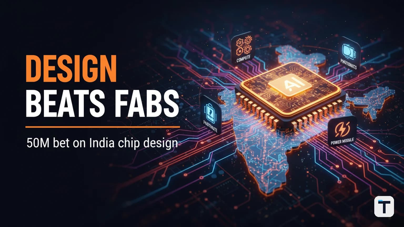

Verdict: Marvell Technology's $250 million, three-year India investment is the cleanest recent signal that the highest-value layer of the AI semiconductor stack is design and IP, not fabrication. The company is doubling an already-large Indian engineering workforce to build custom accelerators, photonics, and power-management silicon for AI infrastructure — and the framing of the bet aligns with how the Indian government itself now talks about its chip strategy. For builders, founders, and operators watching the India semiconductor ecosystem, the takeaway is concrete: the strategy worth copying is the fabless one, where a small team owns the IP and contracts out the silicon.
What is Marvell actually investing $250 million in?
Marvell Technology, Inc. (NASDAQ: MRVL) announced on July 29, 2026 that it will invest $250 million in India over the next three years to expand technology, talent, and infrastructure — timed to mark 20 years of engineering in the country (Marvell Newsroom). The announcement came alongside the inauguration of a new wing at its Bangalore office and an expansion in Hyderabad, with a stated plan to double its India headcount over the same period.
This is not a fabrication play. It is investment in chip design capacity — Marvell describes the spend as funding "the design and development of advanced semiconductor solutions for AI, cloud and data infrastructure applications" (Marvell Newsroom). India already operates as Marvell's second-largest R&D organization worldwide, with teams across Bangalore, Pune, and Hyderabad working on advanced process nodes (down to 2nm and beyond), high-speed analog IP, subsystem design, software/firmware, and end-to-end silicon development.
In other words: the dollars buy engineering brains, EDA tool licenses, labs, and research partnerships — not clean rooms. That distinction matters, and it is the spine of this article.
Why is Marvell betting on India specifically for AI chips?
India's role in Marvell's footprint is a useful case study in how multinationals are quietly rebalancing the semiconductor map. Three structural reasons make the country attractive for AI silicon design work, and they map closely onto what Marvell is doing:
A deep, low-cost design talent pool. India hosts roughly 20% of the global semiconductor design workforce (Invest India), giving companies like Marvell an unusually large bench of engineers skilled in chip architecture, verification, and IP development. Doubling an already-substantial Indian R&D headcount is operationally realistic in a way that it is not in most other geographies.
Government policy is explicitly pro-design. India's Design Linked Incentive (DLI) Scheme, launched in December 2021 under the Semicon India Programme, reimburses up to 50% of eligible design expenditure capped at ₹15 crore per application and pays a deployment-linked incentive of 6%–4% of net sales over five years, capped at ₹30 crore (PIB / MeitY, Jan 2026). The just-approved Semicon 2.0 — a ₹1,27,500 crore fiscal outlay — keeps design as one of its six strategic pillars alongside fabs, ATMP/OSAT, materials, R&D, and talent (India Semiconductor Mission). The policy environment is openly tilted toward fabless.
Proximity to a large inference market. Marvell's own framing is that the Indian AI inference use case will be different from the West's — used across "a billion lives" in education, agriculture, medical, and governance, and therefore priced in rupees per second, not dollars per second. Building custom accelerators locally keeps the design team close to that cost-sensitivity reality, which is exactly the design constraint that drives architecture decisions.
AI infrastructure is bigger than GPUs — what Marvell is actually building
The single most under-reported thing about the AI semiconductor story is that GPUs are only one tile in the mosaic. An AI rack is now an integrated system of compute (GPUs, XPUs, custom ASICs), interconnects and switches, optical networking, memory, storage, power delivery, and security — and every one of those layers is a design problem Marvell works on.
That framing is why Marvell's investment is more strategically interesting than another "BigCo invests in India" headline. Here is what the company is actually working on inside the AI infrastructure envelope, based on its own public statements:
| Layer | What it does | Why it matters for AI racks |
|---|---|---|
| Custom accelerators / XPUs | Application-specific silicon for inference and training workloads | Power- and cost-optimized for specific use cases (India's rupee-per-second model) |
| Co-packaged optics & photonics | Moves data with light instead of copper, integrated into the switch package | Required to break the bandwidth–power wall as scale-out networks exceed electrical limits |
| Switching & interconnects | High-speed data movement between GPUs, XPUs, memory, and storage | Bottleneck shifts from compute to the network at scale; this is where rack performance is won |
| Power management silicon | Steps down 800V from the power line to 48V to 2V and below to feed the racks | AI racks now pull so much power that delivery, not generation, is the constraint |
| Storage, memory, security | Surrounding system IP for the data path | Required for a complete system SKU; also a margin and differentiation layer |
The reason this matters is that AI infrastructure has become a system problem, not a components problem. Power delivery alone is becoming one of the binding constraints as GPUs pull more watts per rack than a small neighborhood. Marvell's bet is that you win this market by owning the IP across several of these layers and partnering for the rest — which is exactly the model it applies with ecosystem partners in India (power-management companies, photonics startups, and academia).
The partners and academic network Marvell is using in India
Building custom accelerators in India is not a Marvell-only exercise — the company is explicitly stitching together an ecosystem rather than trying to vertically integrate. Three patterns are worth flagging because they reveal how a fabless-first strategy scales:
University partnerships for long-horizon R&D. Marvell has set up a large lab at IIT Hyderabad with roughly a dozen active research projects spanning hardware, software, accelerators, and networking. It is replicating the model elsewhere: test facilities at IIT Tirupati, advanced packaging at IIT Bombay, analog mixed-signal design at IIT Madras, and photonics and networking at IISc, with continuing partnerships at institutes like VIT and MIT for design-skills pipeline development.
Ecosystem partnerships for the layers Marvell does not own. Marvell partners with companies that own adjacent pieces — a power-management firm that takes 800V down to 48V and then 2V, and a photonics firm whose IP complements Marvell's for co-packaged optics — then integrates into a system-level sell. That is textbook fabless: own your IP, partner for everything else, win at the system level.
Startup engagement through Semicon 2.0. The newly approved Semicon 2.0 framework is expected to let multinationals participate in DLI and support startups directly — a path Marvell has signaled it intends to use. As of January 2026, DLI already supports 24 chip-design startups with 16 tape-outs, six chips fabricated at advanced nodes, and 10 patents filed, and the programme's stated next target is 50 fabless semiconductor companies (PIB, Jan 2026).
Why Marvell's framing echoes India's own semiconductor strategy
The single most useful idea in the Marvell announcement is one that the Indian government has separately arrived at: design and IP capture more of the semiconductor value chain than manufacturing does. Three data points make the case:
- Semiconductor design contributes up to 50% of value addition and 20–50% of bill-of-materials cost, and the fabless segment accounts for 30%+ of global semiconductor sales (PIB / MeitY, Jan 2026).
- The most valuable semiconductor companies in the world are fabless — Nvidia, Qualcomm, Broadcom, and AMD do not own their own leading-edge fabs. Their margins sit in the design layer; the manufacturing layer is a comparatively thin service.
- The Indian government's own narrative — articulated publicly and reflected in the Semicon 2.0 pillar structure — is that design must come first, because building fabs without owning the IP simply relocates a low-margin link of a chain that someone else controls.
This is the information-gain point of the whole story: an investment like Marvell's is not a substitute for a fab. It is a bet that the next decade's most valuable chip companies will look like today's fabless leaders — design-led, IP-rich, ecosystem-partnered — and that India can produce some of them. For a country that already has the design workforce, the lowest-cost path to a globally competitive semiconductor position is to double down on design and let demand for fabrication follow.
What this means for you
The Marvell bet is not abstract if you are building, investing, or operating in the AI infrastructure space. Three concrete reads:
- For founders and engineers in India: the accessible opportunity is fabless IP, not fabs. Design capability, mixed-signal IP, custom accelerators for vertical use cases (agriculture, medical, governance, education), and photonics are all open lanes — and the DLI scheme will help fund the first leg. The Tamcom-style "build a chip and sell to the world" path is now policy-supported.
- For buyers and operators of AI infrastructure: pay attention to the system-level integrators. As AI racks scale, the constraint is moving from compute to power delivery and networking. Vendors that own IP across multiple layers of the stack — the Marvell model — are better positioned than single-component suppliers to ship complete, cost-optimized systems, especially for cost-sensitive deployments.
- For investors watching the India semiconductor thesis: the high-margin, capital-light part of the India chip story is the design layer, not the manufacturing layer. The ₹1,27,500 crore Semicon 2.0 outlay includes substantial fab and ATMP incentives, but the disproportionate value capture — and the venture-style return profile — sits with the fabless startups supported under DLI and the multinationals that anchor their design center in India.
For a related deep dive on India's broader electronics story (and whether the country is actually replacing China), see our earlier analysis: India's ₹13 lakh crore electronics boom: is India actually replacing China?. For how the same rupee-per-second cost logic plays out at the AI software layer, our AI token cost optimization guide for enterprises walks through the routing and budgeting patterns that mirror the hardware-side economics here.
The honest limits of the bet
A few caveats keep this from being a victory lap. First, $250 million over three years is meaningful but modest in absolute semiconductor terms — Nvidia's quarterly capex dwarfs it — and Marvell's investment is a workforce-and-tools bet, not a leading-edge capacity bet. Second, doubling headcount assumes the Indian design talent pool continues to expand at the needed rate; the Chips to Startup (C2S) programme has trained about 67,000 of a 85,000 ten-year target, which leaves the pipeline tight in the short term (PIB, Jan 2026). Third, the fabless economic argument depends on continued access to leading-edge foundries (TSMC, Samsung) — geopolitical disruption to that access would weaken the model regardless of how strong India's design layer becomes.
None of these caveats erase the core read. They simply bound it: Marvell's $250 million is a deliberate, well-aimed bet on the highest-margin layer of the AI semiconductor stack, in the country with the deepest design talent pool and the most pro-design policy. The shape of the bet is more important than its size.
FAQ
Q: How much is Marvell investing in India? A: Marvell announced a $250 million investment in India over three years on July 29, 2026, timed to its 20th anniversary in the country. The money funds chip-design capacity — tools, labs, talent, and ecosystem partnerships — not a fab, and the plan includes doubling the Indian workforce over the same period (Marvell Newsroom).
Q: Is Marvell building a chip factory in India? A: No. Marvell is a fabless data infrastructure semiconductor company, and its India investment is entirely in design and R&D — including a new Bangalore office wing and Hyderabad expansion. The design work covers advanced process nodes down to 2nm and beyond, but the actual silicon fabrication is contracted out to foundries, as is standard for fabless companies.
Q: Why is India attractive for semiconductor design work? A: India holds roughly 20% of the global semiconductor design workforce, the government's Design Linked Incentive (DLI) scheme reimburses up to 50% of design expenditure, and the newly approved Semicon 2.0 programme (₹1,27,500 crore outlay) keeps design as one of its six strategic pillars. Combined with proximity to a large, cost-sensitive AI inference market, that makes India a strong base for design-led chip companies.
Q: What is the Design Linked Incentive (DLI) scheme? A: DLI is a MeitY scheme launched in December 2021 that reimburses up to 50% of eligible design expenditure (capped at ₹15 crore per application) and pays a deployment-linked incentive of 6%–4% of net sales for five years (capped at ₹30 crore). As of January 2026, it supports 24 chip-design startups, with 16 tape-outs, six chips fabricated at advanced nodes, and a stated target of scaling to 50 fabless firms (PIB, Jan 2026).
Q: Why is fabless chip design more valuable than manufacturing? A: Semiconductor design contributes up to 50% of value addition in the electronics value chain and accounts for 30%+ of global semiconductor sales via the fabless segment. The world's most valuable semiconductor companies (Nvidia, Qualcomm, Broadcom, AMD) are fabless — they own the IP and contract out manufacturing, capturing the high-margin design layer while fabs operate on comparatively thin service economics (PIB / MeitY).
Q: What is Semicon 2.0 and how does it differ from Semicon 1.0? A: Semicon 2.0 is the second phase of India's Semicon India Programme, approved by the Union Cabinet in July 2026 with a fiscal outlay of ₹1,27,500 crore (vs ₹76,000 crore for Semicon 1.0). It is structured around six strategic pillars — design, machines and materials, fabs, ATMP/OSAT, R&D, and talent development — and explicitly broadens the ecosystem focus beyond fabrication to include design, materials, and R&D (India Semiconductor Mission).
Discussion
0 comments